Samsung Unveils Exynos 2600 Chipset for Galaxy S26 Series
Best deals in Nepal
Finding the best deals
Checking stores across Nepal for live prices.
Key Takeaways
- Exynos 2600 built on Samsung's first-gen 2nm GAA process with modest performance gains
- Features deca-core CPU with Arm v9.3 architecture and upgraded NPU for on-device AI
- Set to power Galaxy S26 and S26+ in Europe, while S26 Ultra uses Snapdragon 8 Elite Gen 5 globally
- Supports up to 320MP camera sensors and 8K video playback
- Current yield rates at 60%, deemed sufficient for mass production
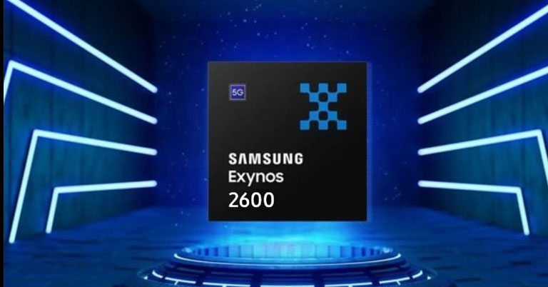
Samsung has officially launched the Exynos 2600, its flagship chipset designed for the 2026 Galaxy S26 and S26+ series. Built using Samsung's first-generation 2nm Gate-All-Around (GAA) process, the processor delivers around a 5% performance boost, an 8% improvement in efficiency, and a 5% reduction in chip size compared to the company’s second-generation 3nm node. Despite these incremental advances, the focus of the 2nm process appears to be on better transistor control, lower leakage, and more stable power delivery rather than dramatic performance leaps.
The Exynos 2600 features a deca-core CPU based on Arm v9.3 architecture, comprising one high-performance C1-Ultra core, three C1-Pro performance cores, and six efficiency-tuned middle cores. Samsung has moved away from traditional “little” cores entirely. The company claims meaningful improvements in computing performance and power consumption, driven by architectural changes and support for newer instruction sets that enhance on-device machine learning responsiveness. While it may not surpass Qualcomm’s Oryon cores in raw benchmark scores, this approach suggests an effort to balance sustained performance with efficiency in a novel way.
AI plays a central role in the Exynos 2600, with an upgraded Neural Processing Unit (NPU) designed to accelerate generative AI tasks while reducing power consumption and latency. Samsung aims to enable more complex AI features, such as advanced image editing and intelligent assistance, to run directly on the device rather than relying heavily on cloud processing. This could allow the Exynos lineup to differentiate itself beyond traditional CPU and GPU metrics.
The chip incorporates the Xclipse 960 GPU, offering improved ray tracing support and AI-based upscaling through ENSS technology. Rather than pursuing maximum frame rates, Samsung seems to prioritize smooth gameplay within limited power budgets. To address thermal challenges—a long-standing issue for Exynos chips—the design includes a new Heat Path Block thermal solution intended to enhance heat dissipation efficiency.
Camera and multimedia capabilities are also noteworthy. The Exynos 2600 supports camera sensors up to 320 megapixels and includes advanced video noise reduction along with 8K video playback capabilities.
Current yield rates for the Exynos 2600 are reported at around 60%, which Samsung considers adequate for mass production. The company has secured approximately 25% of the chip orders for the Galaxy S26 series, with Qualcomm supplying the remaining share, primarily for the Ultra model. Beyond smartphones, Samsung’s early 2nm manufacturing capability is evidenced by a reported $16.5 billion deal with Tesla for AI6 chips, signaling strong confidence in its GAA process despite the two-tier smartphone strategy that will likely continue in certain regions.
The Exynos 2600 is expected to make its debut in the Galaxy S26 and S26+ when these devices launch in 2026. European consumers are likely to receive models powered by the Exynos 2600, while the Galaxy S26 Ultra will utilize the Snapdragon 8 Elite Gen 5 globally.
Key specs
| Process | 2nm GAA |
| Npu | Upgraded for generative AI tasks |
| Video Support | 8K playback |
| Camera Support | Up to 320MP sensors |
| CPU Architecture | Arm v9.3 |
| CPU Cores | Deca-core (1x C1-Ultra, 3x C1-Pro, 6x efficiency cores) |
Want to compare this device with others?
Compare